IBM and Siemens collaborate to advance 3D nanostack technology - Engineering.com
This story deserves to be shared
Send it to someone who'd care, or post it on your networks.

The companies will develop virtual models, simulation and lithography techniques to address fabrication challenges and prepare the architecture for production.
IBM announced new research aimed at advancing IBM’s nanostack architecture, a new transistor architecture unveiled by IBM earlier this year. The collaboration will bring together IBM’s leadership in semiconductor device innovation and Siemens’ expertise in electronic design automation (EDA), process simulation, lithography optimization, and advanced manufacturing software to accelerate the development of nanostack.
This article is an excerpt. To read the full content, visit the original source. Engineering.com
Related articles
ORNL and Mazak collaborate for WAAM platform - Canadian Metalworking
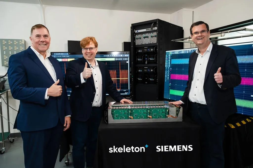
Siemens invests in Skeleton Technologies expanding its data center portfolio - Siemens press
Press Release14 October 2026Smart InfrastructureMunichSiemens is expanding its data center portfolio through a strategic investment and exclusive partnership with

USask collaborates with Siemens, Microchip Technology, and Mitacs to help build Canada’s future semiconductor workforce - University of Saskatchewan
By bringing together academia, industry and government-supported innovation, unique partnerships are giving University of Saskatchewan students hands-on experience while strengthening Canada’s semiconductor talent pipeline. Semiconductors are the foundation of major technology trends shaping the world today, including AI, communications, industrial automation, aerospace, and automotive innovation

Today’s NYT Strands Hints, Spangram and Answers for Sunday, Oct. 18, #959 - CNET
Here’s your NYT Strands hint for today, plus the spangram and all of today’s Strands answers for puzzle No. 959 on Sunday, Oct. 18, 2026. Today’s Strands theme was tricky. It helps to be a runner. Read on for all the answers.
0 comments
No comments yet. Be the first to share your thoughts!